Motherboard:
The main circuit board of a microcomputer. The motherboard contains the connectors for attaching additional boards. Typically, the motherboard contains the CPU, BIOS, memory, mass storage interfaces, serial and parallel ports, expansion slots, and all the controllers required to control standard peripheral devices, such as the display screen, keyboard, and disk drive. Collectively, all these chips that reside on the motherboard are known as the motherboard's chipset.

IBM's Released PC Motherboard - 8088 in the year 1981

The 80286 Motherboard having ISA & EISA Slots
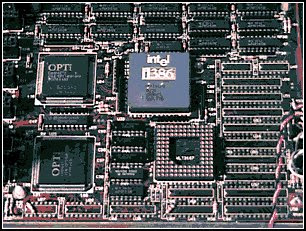
Intel 30386 Motherboard with OPTi Chipset
 80486 Motherboard (Microprocessor used: AMD-486) for Intel Chipset Compatible

80486-(Cyrix Processor) Motherboard
 Pentium-I(Socket-7) Motherboard Layout
Pentium-II (Slot-1) Motherboard Layout

Pentium-III (Slot-1) Motherboard Description
 Pentium-III(Socket-370 FPGA) Motherboard
 Pentium-IV (Intel Chipset) Motherboard
EVOLUTION OF MICRO PROCESSORS IN PCs
It is interesting to note that the microprocessor had existed for only 10 years prior to the creation of the PC! Intel invented the microprocessor in 1971; the PC was created by IBM in 1981. Now more than 20 years later, we are still using systems based more or less on the design of that first PC. The processors powering our PCs today are still backward compatible in many ways with the 8088 that IBM selected for the first PC in 1981.
It is interesting to note that the microprocessor had existed for only 10 years prior to the creation of the PC! Intel invented the microprocessor in 1971; the PC was created by IBM in 1981. Now more than 20 years later, we are still using systems based more or less on the design of that first PC. The processors powering our PCs today are still backward compatible in many ways with the 8088 that IBM selected for the first PC in 1981.
November 15, 2001 marked the 30th anniversary of the microprocessor, and in those 30 years processor speed has increased more than 18,500 times (from 0.108MHz to 2GHz).The 4004 was introduced on November 15, 1971 and originally ran at a clock speed of 108KHz (108,000 cycles per second, or just over one-tenth a megahertz). The 4004 contained 2,300 transistors and was built on a 10-micron process. This means that each line, trace, or transistor could be spaced about 10 microns (millionths of a meter) apart. Data was transferred 4 bits at a time, and the maximum addressable memory was only 640 bytes. The 4004 was designed for use in a calculator but proved to be useful for many other functions because of its inherent programmability. For example, the 4004 was used in traffic light controllers, blood analyzers, and even in the NASA Pioneer 10 deep space probe!
In April 1972, Intel released the 8008 processor, which originally ran at a clock speed of 200KHz (0.2MHz). The 8008 processor contained 3,500 transistors and was built on the same 10-micron process as the previous processor. The big change in the 8008 was that it had an 8-bit data bus, which meant it could move data 8 bits at a timetwice as much as the previous chip. It could also address more memory, up to 16KB. This chip was primarily used in dumb terminals and general-purpose calculators.
The next chip in the lineup was the 8080, introduced in April 1974, running at a clock rate of 2MHz. Due mostly to the faster clock rate, the 8080 processor had 10 times the performance of the 8008. The 8080 chip contained 6,000 transistors and was built on a 6-micron process. Similar to the previous chip, the 8080 had an 8-bit data bus, so it could transfer 8 bits of data at a time. The 8080 could address up to 64KB of memory, significantly more than the previous chip.
It was the 8080 that helped start the PC revolution because this was the processor chip used in what is generally regarded as the first personal computer, the Altair 8800. The CP/M operating system was written for the 8080 chip, and Microsoft was founded and delivered its first product: Microsoft BASIC for the Altair. These initial tools provided the foundation for a revolution in software because thousands of programs were written to run on this platform.
In fact, the 8080 became so popular that it was cloned. A company called Zilog formed in late 1975, joined by several ex-Intel 8080 engineers. In July 1976, it released the Z-80 processor, which was a vastly improved version of the 8080. It was not pin compatible but instead combined functions such as the memory interface and RAM refresh circuitry, which enabled cheaper and simpler systems to be designed. The Z-80 also incorporated a superset of 8080 instructions, meaning it could run all 8080 programs. It also included new instructions and new internal registers, so software designed for the Z-80 would not necessarily run on the older 8080. The Z-80 ran initially at 2.5MHz (later versions ran up to 10MHz) and contained 8,500 transistors. The Z-80 could access 64KB of memory.
RadioShack selected the Z-80 for the TRS-80 Model 1, its first PC. The chip also was the first to be used by many pioneering systems, including the Osborne and Kaypro machines. Other companies followed, and soon the Z-80 was the standard processor for systems running the CP/M operating system and the popular software of the day.
Intel released the 8085, its follow-up to the 8080, in March 1976. Even though it predated the Z-80 by several months, it never achieved the popularity of the Z-80 in personal computer systems. It was popular as an embedded controller, finding use in scales and other computerized equipment. The 8085 ran at 5MHz and contained 6,500 transistors. It was built on a 3-micron process and incorporated an 8-bit data bus.
Along different architectural lines, MOS Technologies introduced the 6502 in 1976. This chip was designed by several ex-Motorola engineers who had worked on Motorola's first processor, the 6800. The 6502 was an 8-bit processor like the 8080, but it sold for around $25, whereas the 8080 cost about $300 when it was introduced. The price appealed to Steve Wozniak, who placed the chip in his Apple I and Apple II designs. The chip was also used in systems by Commodore and other system manufacturers. The 6502 and its successors were also used in game consoles, including the original Nintendo Entertainment System (NES) among others. Motorola went on to create the 68000 series, which became the basis for the Apple Macintosh line of computers. Today those systems use the PowerPC chip, also by Motorola and a successor to the 68000 series.
All these previous chips set the stage for the first PC processors. Intel introduced the 8086 in June 1978. The 8086 chip brought with it the original x86 instruction set that is still present in current x86-compatible chips such as the Pentium 4 and AMD Athlon. A dramatic improvement over the previous chips, the 8086 was a full 16-bit design with 16-bit internal registers and a 16-bit data bus. This meant that it could work on 16-bit numbers and data internally and also transfer 16 bits at a time in and out of the chip. The 8086 contained 29,000 transistors and initially ran at up to 5MHz.
The chip also used 20-bit addressing, so it could directly address up to 1MB of memory. Although not directly backward compatible with the 8080, the 8086 instructions and language were very similar and enabled older programs to quickly be ported over to run. This later proved important to help jumpstart the PC software revolution with recycled CP/M (8080) software.
Although the 8086 was a great chip, it was expensive at the time and more importantly required expensive 16-bit board designs and infrastructure to support it. To help bring costs down, in 1979 Intel released what some called a crippled version of the 8086 called the 8088. The 8088 processor used the same internal core as the 8086, had the same 16-bit registers, and could address the same 1MB of memory, but the external data bus was reduced to 8 bits. This enabled support chips from the older 8-bit 8085 to be used, and far less expensive boards and systems could be made. These reasons are why IBM chose the 8088 instead of the 8086 for the first PC.
This decision would affect history in several ways. The 8088 was fully software compatible with the 8086, so it could run 16-bit software. Also, because the instruction set was very similar to the previous 8085 and 8080, programs written for those older chips could be quickly and easily modified to run. This enabled a large library of programs to be quickly released for the IBM PC, thus helping it become a success. The overwhelming blockbuster success of the IBM PC left in its wake the legacy of requiring backward compatibility with it. To maintain the momentum, Intel has pretty much been forced to maintain backward compatibility with the 8088/8086 in most of the processors it has released since then.
To date, backward compatibility has been maintained, but innovating and adding new features has still been possible. One major change in processors was the move from the 16-bit internal architecture of the 286 and earlier processors to the 32-bit internal architecture of the 386 and later chips, which Intel calls IA-32 (Intel Architecture, 32-bit). Intel's 32-bit architecture dates to 1985, and it took a full 10 years for both a partial 32-bit mainstream OS (Windows 95) as well as a full 32-bit OS requiring 32-bit drivers (Windows NT) to surface, and another 6 years for the mainstream to shift to a fully 32-bit environment for the OS and drivers (Windows XP). That's a total of 16 years from the release of 32-bit computing hardware to the full adoption of 32-bit computing in the mainstream with supporting software. I'm sure you can appreciate that 16 years is a lifetime in technology.
Now we are in the midst of another major architectural jump, as Intel and AMD are in the process of moving from 32-bit to 64-bit computing for servers, desktop PCs, and even portable PCs. Intel had introduced the IA-64 (Intel Architecture, 64-bit) in the form of the Itanium and Itanium 2 processors several years earlier, but this standard was something completely new and not an extension of the existing 32-bit technology. IA-64 was first announced in 1994 as a CPU development project with Intel and HP (codenamed Merced), and the first technical details were made available in October 1997. The result was the IA-64 architecture and Itanium chip, which was officially released in 2001.
The fact that the IA-64 architecture is not an extension of IA-32 but is instead a whole new and completely different architecture is fine for non-PC environments such as servers (for which IA-64 was designed), but the PC market has always hinged on backward compatibility. Even though emulating IA-32 within IA-64 is possible, such emulation and support is slow.
With the door now open, AMD seized this opportunity to develop 64-bit extensions to IA-32, which it calls AMD64 (originally known as x86-64). Intel eventually released its own set of 64-bit extensions, which it calls EM64T or IA-32e mode. As it turns out, the Intel extensions are almost identical to the AMD extensions, meaning they are software compatible. It seems for the first time that Intel has unarguably followed AMD's lead in the development of PC architecture.
To make 64-bit computing a reality, 64-bit operating systems and 64-bit drivers are also needed. Microsoft began providing trial versions of Windows XP Professional x64 Edition (which supports AMD64 and EM64T) in April 2005, and major computer vendors now offer systems with Windows XP Professional x64 already installed. Major hardware vendors have also developed 64-bit drivers for current and recent hardware. Linux is also available in 64-bitcompatible versions, making the move to 64-bit computing possible.
The latest development is the introduction of dual-core processors from both Intel and AMD. Dual-core processors have two full CPU cores operating off of one CPU packagein essence enabling a single processor to perform the work of two processors. Although dual-core processors don't make games (which use single execution threads and are usually not run with other applications) play faster, dual-core processors, like multiple single-core processors, split up the workload caused by running multiple applications at the same time. If you've ever tried to scan for viruses while checking email or running another application, you've probably seen how running multiple applications can bring even the fastest processor to its knees. With dual-core processors available from both Intel and AMD, your ability to get more work done in less time by multitasking is greatly enhanced. Current dual-core processors also support AMD64 or EM64T 64-bit extensions, enabling you to enjoy both dual-core and 64-bit computing's advantages.
PCs have certainly come a long way. The original 8088 processor used in the first PC contained 29,000 transistors and ran at 4.77MHz. The AMD Athlon 64FX has more than 105 million transistors, while the Pentium 4 670 (Prescott core) runs at 3.8GHz and has 169 million transistors thanks to its 2MB L2 cache. Dual-core processors, which include two processor cores and cache memory in a single physical chip, have even higher transistor counts: The Intel Pentium D processor has 230 million transistors, and the AMD Athlon 64 X2 includes over 233 million transistors. As dual-core processors and large L2 caches continue to be used in more and more designs, look for transistor counts and real-world performance to continue to increase. And the progress doesn't stop there because, according to Moore's Law, processing speed and transistor counts are doubling every 1.52 years.
In 1978, Intel introduced the first major processor for personal computers—the 8086—which had a 16-bit data bus, 16-bit registers, and a 20-bit address bus. A 20- bit address bus meant that the 8086 could access 1MB of RAM. The speed of the 8086 ranged from 4.77 MHz to around 10 MHz, which is extremely slow considering today’s standards (approximately 1.5 GHz).
8088
The 8086 chip was too expensive for PC manufacturers to use in their systems and still sell the system at a reasonable price to their customers. So Intel introduced the cheaper 8088 chip a year after the 8086. Like the 8086, the 8088 processor had 16- bit registers and a 20-bit address bus (which meant it could access 1MB of RAM). However, the data bus was decreased from 16-bits to 8-bits. The 8088 ran at the same speed as the 8086, keeping its speeds at 4.77 MHz and 8 MHz. The 8086/8088 did not include a built-in cache, nor did it have a built-in math co-processor. If you wanted to add a math co-processor to your system, you would purchase an 8087 chip to sit on the system board beside the CPU. The 8087 chip was specifically designed as the math co-processor for the 8086 and 8088 processors.
80286
In 1982, Intel produced the 80286 chip, which had 16-bit registers and a 16-bit data bus, and ran at speeds ranging between 6 MHz and 20 MHz. Other than the speed increase, these characteristics matched that of the 8086—this time, however, the market was there. The 80286 also increased the size of the address bus to 24-bits, which meant that it could access up to 16MB of RAM. Like the 8086/8088, the 80286 processor did not contain its own internal cache, nor did it include a math co-processor. Processors prior to the 80286 chip ran in real mode, while the 80286 processor introduced what is known as protected mode. The following sections compare real mode with protected mode.
Real mode
Real mode meant that the processor accessed memory as a whole and dealt with it as a single entity. In other words, real-mode processors did not have any multitasking capabilities—the capacity to divide memory up into multiple parts and run a different application (or task) in each part, switching back and forth between them.
Protected mode
Protected-mode processors support the dividing up of system memory into different parts and assigning a different application to each part of memory. Therefore, protected-mode processors support multitasking and multitasking operating systems, such as Windows 95/98, Windows NT, and Windows 2000. Protected-mode processors also support virtual memory, which is the process of using hard disk space as emulated memory. This means you could have 2MB of RAM while the system is also using 10MB of hard disk space as “pretend” RAM. In this case—as far as the applications that are running are concerned—there is 12MB of RAM.
80386DX
In 1985, Intel released its first 32-bit processor, the 80386DX, which had a 32-bit data bus, a 32-bit address bus, and 32-bit registers. The 32-bit address bus meant that the 80386DX processor could access 4 gigabytes (GB) of RAM, which is an amazing improvement over previous processors (unfortunately, most people can’t afford to purchase 4 GB of RAM).
The speed of the 80386DX processor ranged between 16 MHz and 40 MHz. The 80386DX contains no built-in cache, and the math co-processor (the 80387 chip) has to be purchased separately. Once again, the math co-processor would be inserted on the system board in the math co-processor socket.
80386SX
Three years after the 80386DX chip was out, Intel released the 80386SX, which was a lower-end 386 chip. The 80386SX was a 16-bit processor, meaning it had a 16-bit data bus. It could also only access 16MB of RAM, so the address bus had been reduced to 24-bit. The speed of the 80386SX processor ranged from 16 MHz to 33 MHz. The registers were maintained as 32-bit registers.
Although both flavors of the 80386 chips support real and protected mode, they have taken this support to the next level. These chips enable on-the-fly switching between the two modes, whereas the 80286 processor had to be reset before it could switch from one mode to another.
The major difference between the 80386DX processor and the 80386SX processor is that the DX flavor is a 32-bit processor, while the SX flavor is a 16-bit processor. When you compare the characteristics of the 80286 and the 80386SX chip, you realize that the 80286 chip is competitive with the 80386SX chip. In reality, an 80386SX chip is nothing more than a glorified 80286 chip with a bigger price tag.
80486DX
In 1989, major advancements were made in the performance of the computer system when Intel released the 80486DX chip. This chip had a 32-bit data bus, a 32-bit address bus (4GB of RAM), and 32-bit registers.
The 80486DX chip introduced two major advancements in CPU technology. The first was the idea of integrating cache directly into the chip. The 80486DX had 8 kilobytes (K) of built-in cache, or what is called L1 cache. The second major advancement was that the math co-processor was integrated inside the 80486DX chip. Now, instead of buying a math co-processor chip and inserting it onto the system board, the chip was integrated and working as long as it was enabled in the system BIOS. The speed of the 80486DX ranged from 20 MHz to 50 MHz (20 MHz, 25 MHz, and 33 MHz were the most popular speeds). After the original 486s, a second generation of the 80486DX arrived that were marketed as 80486DX2-50, 80486DX2-66, and 80486DX4-100. The following sections discuss the DX2 and DX4 model processors.
80486DX2
The “80486DX” portion of “80486DX2-50” means that the processor is the DX flavor of the 80486. The “2” after the “DX” implies “clock double,” a term indicating that the CPU is working at twice the speed of the system board. In our example, the CPU works at a speed of 50 MHz, while the system board runs at 25 MHz. So, as information travels out of the CPU and hits the system board, the data slows down to half the speed. The same could be said for the 80486DX2-66. The CPU works at a speed of 66 MHz, while the system board runs at 33 MHz.
80486DX4
The DX4 model works exactly the same way as the clock double, only the clock double is actually a clock triple. In other words, the CPU works at three times the speed of the system board. So, why call it a “DX4” if it’s really a clock triple? Because one extra enhancement, other than the clock triple, was added to the DX4: 8K more of L1 cache to the chip. The idea is that our clock triple plus the extra 8K of cache memory gives us a DX4 chip: (clock)3 plus 8(K) equals (DX)4. All 80486 chips—except the DX4 chips, which have 16K of L1 cache—have 8K of L1 cache. Also, all processors created after the 80486 chip use L1 cache, though they may differ in the actual amount. This becomes one of the selling points of the different processors.
80486SX
Two years after the success of the 80486DX chip, Intel decided to market a lowerend 80486 chip. This new chip, released in 1991, was called the 80486SX. What did the 80486SX chip have that made it so special? Or maybe a better question to ask is: What didn’t it have? The 80486SX chip was a full-blown 80486DX with the integrated math co-processor disabled. This time, Intel was trying to attract customers who could not justify the price of the more functional chip, so Intel simply downgraded the 80486DX, marketing it as a different chip and selling it at a lower price.
Because the 80486SX chip did not have an integrated and functioning math co-processor, there was a place on the system board to add a math co-processor chip (the 80487SX).
MMX Technology
MMX technology was originally named for multimedia extensions, or matrix math extensions, depending on whom you ask. Intel officially states that it is actually not an abbreviation and stands for nothing other than the letters MMX (not being an abbreviation was apparently required so that the letters could be trademarked); however, the internal origins are probably one of the preceding. MMX technology was introduced in the later fifth-generation Pentium processors as a kind of add-on that improves video compression/decompression, image manipulation, encryption, and I/O processing all of which are used in a variety of today's software.
MMX consists of two main processor architectural improvements. The first is very basic; all MMX chips have a larger internal L1 cache than their non-MMX counterparts. This improves the performance of any and all software running on the chip, regardless of whether it actually uses the MMX-specific instructions.
The other part of MMX is that it extends the processor instruction set with 57 new commands or instructions, as well as a new instruction capability called single instruction, multiple data (SIMD).
Modern multimedia and communication applications often use repetitive loops that, while occupying 10% or less of the overall application code, can account for up to 90% of the execution time. SIMD enables one instruction to perform the same function on multiple pieces of data, similar to a teacher telling an entire class to "sit down," rather than addressing each student one at a time. SIMD enables the chip to reduce processor-intensive loops common with video, audio, graphics, and animation.
Intel also added 57 new instructions specifically designed to manipulate and process video, audio, and graphical data more efficiently. These instructions are oriented to the highly parallel and often repetitive sequences frequently found in multimedia operations. Highly parallel refers to the fact that the same processing is done on many data points, such as when modifying a graphic image. The main drawbacks to MMX were that it worked only on integer values and used the floating-point unit for processing, so time was lost when a shift to floating-point operations was necessary. These drawbacks were corrected in the additions to MMX from Intel and AMD.
Intel licensed the MMX capabilities to competitors such as AMD and Cyrix, who were then able to upgrade their own Intel-compatible processors with MMX technology.
Pentium II Processors
Intel revealed the Pentium II in May 1997. Prior to its official unveiling, the Pentium II processor was popularly referred to by its codename, Klamath, and was surrounded by much speculation throughout the industry. The Pentium II is essentially the same sixth-generation processor as the Pentium Pro, with MMX technology added (which included double the L1 cache and 57 new MMX instructions); however, there are a few twists to the design.
From a physical standpoint, it was a big departure from previous processors. Abandoning the chip in a socket approach used by virtually all processors up until this point, the Pentium II chip is characterized by its SEC cartridge design. The processor, along with several L2 cache chips, is mounted on a small circuit board (much like an oversized-memory SIMM), and the circuit board is then sealed in a metal and plastic cartridge. The cartridge is then plugged into the motherboard through an edge connector called Slot 1, which looks very much like an adapter card slot.
As you can see from these figures, the SECC2 version was cheaper to make because it uses fewer overall parts. It also allowed for a more direct heatsink attachment to the processor for better cooling. Intel transitioned from SECC to SECC2 in the beginning of 1999; all later PII chips, and the Slot 1 PIII chips that followed, use the improved SECC2 design.
By using separate chips mounted on a circuit board, Intel could build thePentium II much less expensively than the multiple die within a package used in the Pentium Pro. Intel could also use cache chips from other manufacturers and more easily vary the amount of cache in future processors compared to the Pentium Pro design.
Intel offered Pentium II processors with the following speeds: (Processor Speed/Clock Speed/Motherboard Speed)
Pentium II 233MHz/3.5x/66MHz
Pentium II 266MHz/4x/66MHz
Pentium II 300MHz/4.5x/66MHz
Pentium II 333MHz/5x/66MHz
Pentium II 350MHz/3.5x/100MHz
Pentium II 400MHz/4x/100MHz
Pentium II 450MHz/4.5x/100MHz
The Pentium II processor core has 7.5 million transistors and is based on Intel's advanced P6 architecture. The Pentium II started out using a 0.35-micron process technology, although the 333MHz and faster Pentium IIs are based on 0.25-micron technology. This enables a smaller die, allowing increased core frequencies and reduced power consumption. At 333MHz, the Pentium II processor delivers a 75%150% performance boost, compared to the 233MHz Pentium processor with MMX technology, and approximately 50% more performance on multimedia benchmarks iCOMP 2.0 Index rating for the Pentium II 266MHz chip is more than twice as fast as a classic Pentium 200MHz.
Aside from speed, the best way to think of the Pentium II is as a Pentium Pro with MMX technology instructions and a slightly modified cache design. It has the same multiprocessor scalability as the Pentium Pro, as well as the integrated L2 cache. The 57 new multimedia-related instructions carried over from the MMX processors and the capability to process repetitive loop commands more efficiently are included as well. Also included as a part of the MMX upgrade is double the internal L1 cache from the Pentium Pro (from 16KB total to 32KB total in the Pentium II).
Pentium III & Pentium II & III Xenon
The Pentium III processor was first released in February 1999 and introduced several new features to the P6 family. It is essentially the same core as a Pentium II with the addition of SSE instructions and integrated on-die L2 cache in the later versions. SSE consists of 70 new instructions that dramatically enhance the performance and possibilities of advanced imaging, 3D, streaming audio, video, and speech-recognition applications.
Originally based on Intel's advanced 0.25-micron CMOS process technology, the PIII core started out with more than 9.5 million transistors. In late 1999, Intel shifted to a 0.18-micron process die (codenamed Coppermine) and added 256KB of on-die L2 cache, which brought the transistor count to 28.1 million. The latest version of the Pentium III (codenamed Tualatin) uses a 0.13-micron process and has 44 million transistors; motherboards made before the Tualatin-core versions of the Pentium III generally do not support this processor because of logical pinout changes. The Pentium III was manufactured in speeds from 450MHz through 1.4GHz, as well as in server versions with larger or faster cache known as the Pentium Xeon. The Pentium III also incorporates advanced features such as a 32KB L1 cache and either half-core speed 512KB L2 cache or full-core speed on-die 256KB or 512KB L2 with cacheability for up to 4GB of addressable memory space. The PIII also can be used in dual-processing systems with up to 64GB of physical memory. A self-reportable processor serial number gives security, authentication, and system management applications a powerful new tool for identifying individual systems. Because of privacy concerns when the processor was released, you can disable this feature in the system BIOS on most systems that use the Pentium III or Celeron III processors.
Pentium III processors were first made available in Intel's SECC2 form factor, which replaced the more expensive older SEC packaging. The SECC2 package covers only one side of the chip and allows for better heatsink attachment and less overall weight. Architectural features of the Pentium III processor include:
· Streaming SIMD extensions (SSE). Seventy new instructions for dramatically faster processing and improved imaging, 3D streaming audio and video, web access, speech recognition, new user interfaces, and other graphics and sound-rich applications.
· Intel processor serial number. The processor serial number serves as an electronic serial number for the processor and, by extension, its system or user. This feature can be enabled or disabled as desired in the BIOS Setup. The serial number enables the system/user to be identified by company internal networks and applications. The processor serial number can be used in applications that benefit from stronger forms of system and user identification, such as:
o Applications using security capabilities. Managed access to new Internet content and services; electronic document exchange.
o Manageability applications. Asset management; remote system load and configuration.
Although the initial release of Pentium III processors was made in the improved SECC2 packaging, Intel later switched to the FC-PGA package, which is even less expensive to produce and enables a more direct attachment of the heatsink to the processor core for better cooling. The FC-PGA version plugs into Socket 370 but can be used in Slot 1 with a slot-ket adapter.
All Pentium III processors have either 512KB or 256KB of L2 cache, which runs at either half-core or full-core speed. Pentium III Xeon versions have 512KB, 1MB, or 2MB of L2 cache that runs at full-core speed. The Pentium III Xeon is a more expensive version of the Pentium III designed for servers and workstations. All PIII processor L2 caches can cache up to 4GB of addressable memory space and include ECC capability.
PIII Processor Speeds: (Processor Speed/Bus Speed/Clock Speed):
450MHz/100/4.5x
500MHz/100/5x
500E/100/5x
533B/133/4x
533EB/133/4x
550MHz/100/5.5x
550E/100/5.5x
600MHz/100/6x
600E/100/6x
600B/133/4.5x
600EB/133/4.5x
650/100/6.5x
667/133/5x
700/100/7x
733/133/5.5x
750/100/7.5x
800MHz/100/8x
800EB/133/6x
850/100/8.5x
866/100/6.5x
900/100/9x
933/133/7x
1000B/133/7.5x
1000MHz/100/10x
1000B/133/7.5x
1100MHz/133/11x
1133MHz/133/8.5x
1200MHz/133/9x
1266MHz/133/9.5x
1333MHz/133/10x
1400MHz/133/10.5x
Pentium II/III Xeon
The Pentium II and III processors were the basis for special high-end versions called Pentium II Xeon (introduced in June 1998) and Pentium III Xeon (introduced in March 1999). Intel now uses the term Xeon by itself to refer to Xeon processors based on the Pentium 4. These differ from the standard Pentium II and III in three ways: packaging, cache size, and cache speed.
Pentium II/III Xeon processors use a larger SEC cartridge than the standard PII/III processors, mainly to house a larger internal board with more cache memory.
Besides the larger package, the Xeon processors also include more L2 cache. They were produced in three variations, with 512KB, 1MB, or 2MB of L2 cache.
Even more significant than the size of the cache is its speed. All the cache in the Xeon processors run at the full-core speed. This is difficult to do considering that the cache chips were separate chips on the board in most versions. The original Pentium II Xeon processors had 7.5 million transistors in the main processor die, whereas the later Pentium III Xeon came with 9.5 million. When the Pentium III versions with on-die cache were released, the transistor count went up to 28.1 million transistors in the 256KB cache version, 84 million transistors in the 1MB cache version, and 140 million transistors in the 2MB cache version, which set an industry record at the time. The high transistor counts are due to the on-die L2 cache, which is very transistor intensive. The L2 cache in all Pentium II and III Xeon processors has a full 64GB RAM address range and supports ECC.
Xeon Processors: CPU Speed/FSB(Bus Speed)
PII Xeon:
400MHz/100MHz,
450MHz/100MHz
PIII Xeon:
500MHz/100MHz,
550/100, 600/133,
667/133, 700/100,
733/133, 800/133,
866/133, 900/100,
933/133, 1000/133.
Xeon:
700MHz/133MHz.
Intel P6(686) Processors:
The P6 (686) processors represent a new generation with features not found in the previous generation units. The P6 processor family began when the Pentium Pro was released in November 1995. Since then, Intel has released many other P6 chips, all using the same basic P6 core processor as the Pentium Pro.
Intel P6 Processors: (Processor Type/ and Features)
Pentium Pro/Original P6 processor, includes 256KB, 512KB or 1MB of full-core speed L2 cache.
Pentium II / P6 with 512KB of half-core speed L2 Cache.
Pentium II Xeon / P6 with 512KB, 1MB or 2MB of full-core speed L2 cache.
Celeron / P6 with no L2 cache.
Celeron-A / P6 with 128KB of on-die full-core speed L2 cache.
Pentium III / P6 with SSE(MMX2), 512KB of half-core speed L2 cache.
Pentium IIPE / P6 with 256Kb of full-core speed L2 cache.
Pentium IIIE / P6 with SSE(MMX2) plus 256KB or 512KB of full-core speed L2 cache.
Pentium III Xeon / P6 with SSE(MMX2), 512KB, 1MB or 2MB of full-core speed L2 cache.
The main new feature in the fifth-generation Pentium processors was the superscalar architecture, in which two instruction execution units could execute instructions simultaneously in parallel. Later fifth-generation chips also added MMX technology to the mix, as well. So then what did Intel add in the sixth generation to justify calling it a whole new generation of chip? Besides many minor improvements, the real key features of all sixth-generation processors are Dynamic Execution and the Dual Independent Bus (DIB) architecture, plus a greatly improved superscalar design.
Dynamic Execution:
Dynamic execution enables the processor to execute more instructions on parallel, so tasks are completed more quickly. This technology innovation is comprised of three main elements:
Multiple branch prediction. Predict the flow of the program through several branches
Dataflow analysis. Schedules instructions to be executed when ready, independent of their order in the original program
Speculative execution:
Increases the rate of execution by looking ahead of the program counter and executing instructions that are likely to be necessary.
Dual Independent Bus:
The other main P6 architecture feature is known as the Dual Independent Bus. This refers to the fact that the processor has two data buses: one for the system (motherboard) and the other just for cache. This enables the cache memory to run at speeds previously not possible.
Other Sixth-Generation Improvements:
Finally, the P6 architecture upgrades the superscalar architecture of the P5 processors by adding more instruction execution units and by breaking down the instructions into special micro-ops. This is where the CISC instructions are broken down into more RISC commands. The RISC-level commands are smaller and easier for the parallel instruction units to execute more efficiently. With this design, Intel has brought the benefits of a RISC processor high-speed dedicated instruction execution to the CISC world. Note that the P5 had only two instruction units, whereas the P6 has at least six separate dedicated instruction units. It is said to be three-way superscalar because the multiple instruction units can execute up to three instructions in one cycle.
Other improvements in efficiency also are included in the P6 architecture: built-in multiprocessor support, enhanced error detection and correction circuitry, and optimization for 32-bit software.
Rather than just being a faster Pentium, the Pentium Pro, Pentium II/III, and other sixth-generation processors have many feature and architectural improvements. The core of the chip is very RISC-like, whereas the external instruction interface is classic Intel CISC. By breaking down the CISC instructions into several RISC instructions and running them down parallel execution pipelines, the overall performance is increased.
Compared to a Pentium at the same clock speed, the P6 processors are faster as long as you're running 32-bit software. The P6 Dynamic Execution is optimized for performance primarily when running 32-bit software, such as Windows NT. If you are using 16-bit software, such as Windows 95 or 98 (which still operate part time in a 16-bit environment) and most older applications, the P6 does not provide as marked a performance improvement over similarly speed-rated Pentium and Pentium-MMX processors. That's because the Dynamic Execution capability is not fully exploited. Because of this, Windows NT/2000/XP often are regarded as the most desirable operating systems for use with Pentium Pro/II/III/ Celeron processors. Although this is not exactly true (a Pentium Pro/II/III/Celeron runs fine under Windows 95/98), Windows NT/2000/XP does take better advantage of the P6's capabilities.
Note that it is really not so much the operating system but which applications you use. Software developers can take steps to gain the full advantages of the sixth-generation processors. This includes using modern compilers that can improve performance for all current Intel processors, writing 32-bit code where possible, and making code as predictable as possible to take advantage of the processor's Dynamic Execution multiple branch prediction capabilities.
CELERON Processors:
The Celeron processor is a chameleon. It was originally a P6 with the same processor core as the Pentium II in the original two versions; later it came with the same core as the PIII; and more recently it has been based on the various the Pentium 4 cores, including Prescott. It is designed mainly for lower-cost PCs.
Most of the features for the Celeron are the same as the Pentium II, III, or 4 because it uses the same internal processor cores. The main differences are in packaging, L2 cache amount, and CPU bus speed.
The first version of the Celeron was available in a package called the single edge processor package (SEPP or SEP package). The SEP package is basically the same Slot 1 design as the SECC used in the Pentium II/III, with the exception of the fancy plastic cartridge cover. This cover was deleted in the Celeron, making it cheaper to produce and sell. Essentially, the original Celeron used the same circuit board as is inside the Pentium II package.
Even without the plastic covers, the Slot 1 packaging was more expensive than it should have been. This was largely due to the processor retention mechanisms (stands) required to secure the processor into Slot 1 on the motherboard, as well as the larger and more complicated heatsinks required. This, plus competition from the lower-end Socket 7 systems using primarily AMD processors, led Intel to introduce the Celeron in a socketed form. The socket is called PGA-370 or Socket 370 because it has 370 pins. The processor package designed for this socket is called the plastic pin grid array (PPGA) packageor flip chip PGA (FC-PGA). Both the PPGA and FC-PGA packages plug into the 370 pin socket and allow for lower-cost, lower-profile, and smaller systems because of the less expensive processor retention and cooling requirements of the socketed processor.
All Celeron processors at 433MHz and lower were available in the SEPP that plugs into the 242-contact slot connector (Slot 1). The 300MHz and higher versions were also made in the PPGA package. This means that the 300MHz to 433MHz have been available in both packages, whereas the 466MHz and higher-speed versions are available only in the PPGA. The fastest Celeron processor for Socket 370 runs at 1.4GHz; faster Celerons use Socket 478 and are based on the Pentium 4 design.
Motherboards that include Socket 370 can accept the PGA versions of both the Celeron and Pentium III in most cases. If you want to use a Socket 370 version of the Celeron in a Slot 1 motherboard, slot-to-socket adapters (usually called slot-kets) are available for about $10$20 that plug into Slot 1 and incorporate a Socket 370 on the card.
Highlights of the Celeron include the following:
· Available at 300MHz (300A) and higher core frequencies with 128KB on-die L2 cache; 300MHz and 266MHz core frequencies without L2 cache
· L2 cache supports up to 4GB RAM address range and ECC
· Uses same P6 core processor as the Pentium II (266MHz through 533MHz), the Pentium III (533A MHz and higher), and the Pentium 4 (1.7GHz and higher)
· Dynamic execution microarchitecture
· Operates on a 66MHz, 100MHz, 400MHz, or 533MHz CPU bus depending on the version
· Specifically designed for lower-cost value PC systems
· Includes MMX technology; Celeron 533A and higher include SSE; Celeron 1.7GHz and higher include SSE2; Celeron D models include SSE3
· More cost-effective packaging technology, including SEP, PPGA, and FC-PGA or FC-PGA2 packages
· Integrated L1 and L2 cache on most models, with amount and type depending on the version; typically, the Celeron has half the L2 cache of the processor core it is patterned after
· Integrated thermal diode for temperature monitoring
The Intel Celeron processors from the 300A and higher include integrated 128KB L2 cache. The core for the 300A through 533MHz versions that are based on the Pentium II core include 19 million transistors because of the addition of the integrated 128KB L2 cache. The 533A and faster versions are based on the Pentium III core and incorporate 28.1 million transistors. The 1.7GHz and faster versions are based on the Pentium 4 core with 42 million transistors. The Pentium III and Pentium 4based versions actually have 256KB of L2 cache on the die; however, 128KB is disabled, leaving 128KB of functional L2 cache. This was done because it was cheaper for Intel to simply make the Celeron using the same die as the Pentium III or 4 and just disable part of the cache on the Celeron versions, rather than coming up with a unique die for the newer Celerons. The Pentium IIIbased Celeron processors also support the SSE in addition to MMX instructions, whereas the Pentium 4based versions support SSE2 instructions. The older Celerons based on the Pentium II core support only MMX.
All the Celerons in SEPP and PPGA form are manufactured using the 0.25-micron process, whereas those in FC-PGA and FC-PGA2 form are made using the better 0.18-micron and 0.13-micron processes. The smaller process reduces processor heat and enables higher speeds.
The latest Celeron processors for desktop computers use the Celeron D brand name, whereas the Celeron M brand name identifies Celeron-class processors designed for use in low-cost portable computers. Celeron D processors are manufactured using the 0.09-micron process.
A Brief Celeron History
The original Celerons were economy versions of the Intel Pentium II processor. Intel figured that by taking a Pentium II and deleting the separate L2 cache chips mounted inside the processor cartridge (and also deleting the cosmetic cover), it could create a "new" processor that was basically just a slower version of the Pentium II. As such, the first 266MHz and 300MHz Celeron models didn't include any L2 cache. Unfortunately, this proved to have far too great a crippling effect on performance, so starting with the 300A versions, the Celeron received 128KB of on-die full-speed L2 cache, which was actually faster and more advanced than the 512KB of half-speed cache used in the Pentium II it was based on! In fact, the Celeron was the first PC processor to receive on-die L2 cache. It wasn't until the Coppermine version of the Pentium III appeared that on-die L2 cache migrated to Intel's main processors.
Needless to say, this caused a lot of confusion in the marketplace about the Celeron. Considering that the Celeron started out as a "crippled" Pentium II and then was revised so as to actually be superior in some ways to the Pentium II on which it was based (all the while selling for less), many didn't know just where the Celeron stood in terms of performance. Fortunately, the crippling lack of L2 cache existed only in the earliest Celeron versions; all of those at speeds greater than 300MHz have on-die full-speed L2 cache.
The earliest Celerons from 266MHz up through 400MHz were produced in a SEPP design that physically looked like a circuit board and that was designed to fit into Slot 1. This is the same slot the Pentium II used, meaning the Celeron SEPP plugged into any Pentium II Slot-1 motherboard. As the Celeron continued to develop, the form factor was changed to correspond with changes in the Pentium II-, III-, and 4-class processors from which it was adapted. Starting with the 300A processor (300MHz Celeron with 128KB of on-die Level 2 cache), Celerons were produced in a PPGA package using the Socket 370 interface. This socket, with differences in voltage, was later used for most versions of the Pentium III. Celerons using Socket 370 range in speed from 300MHz all the way up to 1.4GHz. Along the way, the packaging changed from PPGA to FC-PGA and FC-PGA2. The latter added a metal heat spreader on top of the die offering better protection for the fragile die.
Celeron processors based on the Pentium 4 are produced in one of two package designs. Some use the FC-PGA2 package that fits into the same Socket 478 used by most Pentium 4 processors. However, the Celeron D is available in both the Socket 478 package and Socket T (LGA775) package used by the Prescott core version of the Pentium 4. The Celeron was never produced in the short-lived Socket 423 form factor the original Pentium 4 processors used.
As this very brief history shows, the name Celeron has never meant anything more specific than a reduced-performance version of Intel's current mainstream processor. Before you can decide whether a particular Celeron processor is a suitable choice, you need to know what its features are and especially on which processor it is based. At least eight discrete variations of the Celeron processor exist.
Celeron Version/ Architecture Based / L2 Cache(KB)/ Multimedia Support/Socket Type/ Bus Speed/ CPU Speed(Min-Max speed):
Celeron/P-II/0KB/MMX/Slot-1/66MHz/266MHz-300MHz)
Celeron-A/P-II/128/MMX/Slot-1/66MHz/300-433MHz
Celeron-A-PGA/P-III/128/MMX/Socket-370/66MHz/300-533MHz
Celeron-III/P-III/ 128/SSE/Socket-370/66 or 100MHz/ 533-1.1GHz
Celeron-IIIA/ P-III/ 256/ SSE/ Socket-370/ 100MHz/ 900-1.4GHz
Celeron-4/ P4/128/SSE2/Socket-478/400MHz/1.7GHz-1.8GHz
Celeron-4A/P4/128/SSE2/Socket-478/400MHz/2.0GHz-2.8GHz
Celeron-D/P4/256/SSE3/Socket-478/ Socket T(LGA775)/ 533MHz/2.13GHz-3.33GHz)
Note:
MMX = Multimedia extensions; 57 additional instructions for graphics and sound processing.
SSE = Streaming SIMD (single instruction multiple data) extensions; MMX plus 70 additional instructions for graphics and sound processing.
SSE2 = Streaming SIMD extensions 2; SSE plus 144 additional instructions for graphics and sound processing.
As you can see, there is a wide range of what is called a Celeron, and you could consider the Celeron as a family of different core processor models in several package variations.
The following sections discuss the differences between these Celeron processors.
Socket 370 Celerons
Socket 370 Celerons are based on various versions of the Pentium II and Pentium III architecture.
Intel offered Celeron IIIA versions for Socket 370 motherboards in speeds from 900MHz to 1.4GHz. These processors have a CPU bus speed of 100MHz. Celeron IIIA versions based on the Pentium III Tualatin core have 256KB of L2 cache, whereas those based on the earlier Pentium III Coppermine core or Pentium II Deschutes core have 128KB of L2 cache. Compared to Celerons based on the previous Pentium III Coppermine core, Tualatin-based Celerons have the following differences:
· Larger L2 memory cache (256KB versus 128KB)
· Improved L2 cache design for better performance
· FC-PGA2 packaging, which includes a metal heat spreader over the fragile CPU core to protect it when attaching a heatsink.
Like the Tualatin-core versions of the Pentium III, Celerons based on the Tualatin core don't work in motherboards designed for older Pentium III or Celeron chips. Socket 370 is physically the same, but the Tualatin core redefines 10 pins in the socket, which requires corresponding changes in the chipset and motherboard. So, if you're looking for a way to speed up an older Celeron by installing a Tualatin-core Celeron IIIA, make sure the motherboard is Tualatin-ready. Also note that Tualatin-core Celerons use the FC-PGA2 packaging, which includes a heat spreader on top of the CPU die. This requires a compatible heatsink.
Socket 478 Celeron and Celeron D Processors
Celeron processors in Socket 478 fall into three distinct camps:
· Celerons running at 1.7GHz and 1.8GHz are based on the original Pentium 4 Willamette core and have a 400MHz CPU bus, 128KB of L2 cache, and SSE2 support.
· Celerons running at 2GHz2.8GHz with a 400MHz CPU bus are based on the Pentium 4 Northwood core, have 128KB of L2 cache, and have SSE2 support.
Celeron D processors are based on the Prescott core used by the latest Pentium 4 processors; range in speed from 2.13GHz to 3.2GHz; and feature a 533MHz CPU bus, 256KB of L2 cache, and SSE3 support.
Socket T (LGA 775) Celeron D Processors
Celeron D processors in Socket T (LGA 775) range in speed from 2.53GHz to 3.2GHz and feature a 533MHz CPU bus, 256KB of L2 cache, and SSE3 support just like their Socket 478 Celeron D siblings. However, they also have two unique features compared to Celeron D processors in Socket 478:
· All-feature support for the Execute Disable Bit feature, which helps block buffer overrun virus attacks, when used with a compatible operating system such as Windows XP Service Pack 2.
· Some also feature support for EM64T, Intel's implementation of 64-bit extensions to the IA32 processor architecture. Thus, Celeron D processors with EM64T provide a low-cost way to use 64-bit operating systems such as Windows XP Professional x64 Edition or 64-bit Linux distributions.

3 comments:
There is very clear information. I am sure, this is very useful to everybody. Thaks for sharing.
Oh, I found exact inormation which I've been searching. Wish to see more blogs regarding this. Want to read about I/O architecture and BIOS, hope you will post soon. Thanks for sharing this with public.
There are no updating postings later on 2007 about the new technologies and enhancements or new innovations. It would be great if the author of this blog continue posting.
Posted information is goodenough to learn in easyway for beginners.
Thanking you.
Social Media Marketing 828706834.877147
Post a Comment